Most operational amplifiers arrive as tidy black packages that quietly perform mathematical miracles while revealing almost nothing about the circuitry inside. Connect power, add feedback resistors, and the chip obediently amplifies, filters, integrates, or converts current into voltage. Convenient? Absolutely. Educational? About as transparent as a locked refrigerator.
A discrete MOSFET op amp turns that refrigerator light on. Instead of hiding dozens of transistors inside silicon, the OPM-03 project reduces the essential functions of an operational amplifier to five visible MOSFETs, a handful of resistors, two adjustments, and a compensation capacitor. Its performance cannot compete with a modern precision IC, but that is not the point. The circuit lets builders see how a differential input stage, voltage-gain stage, output buffer, bias network, and negative-feedback loop cooperateand occasionally argueto produce a working amplifier.
Why Build a Discrete Operational Amplifier?
Commercial op amps are astonishingly capable. Precision devices may offer enormous open-loop gain, tiny offset voltage, excellent power-supply rejection, and carefully controlled behavior across temperature. Those achievements depend on closely matched transistors fabricated beside one another on the same die, plus trimming and compensation techniques that are difficult to reproduce with individual components.
Building a discrete op amp is therefore less about outperforming an integrated circuit and more about exposing its internal logic. Every important limitation becomes visible. Input offset can be traced to transistor mismatch. Restricted output swing can be traced to MOSFET threshold voltage. A mysterious high-frequency wiggle can usually be blamed on phase shift, parasitic capacitance, layout, or all three forming a tiny conspiracy.
The MOSFET-based OPM-03 is especially instructive because it follows a classic three-stage structure while using only five active devices. The design consists of an N-channel differential pair, a P-channel voltage-gain transistor, and a complementary source-follower output stage. It is analog design stripped down to its work boots.
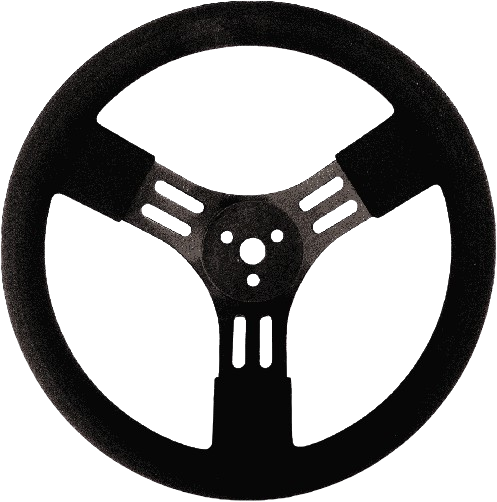
The Five-MOSFET Architecture
Stage One: The MOSFET Differential Pair
The first stage contains two 2N7000 N-channel MOSFETs. Their gates form the non-inverting and inverting inputs. Ideally, when both input voltages are equal, the two devices share current equally and produce a balanced output. When one gate rises slightly above the other, current shifts between the two branches. That small difference becomes the raw error signal that drives the rest of the amplifier.
This is the heart of an op amp. It does not primarily amplify either input voltage relative to ground; it responds to the difference between them. Signals appearing equally on both inputs should largely cancel. That ability is called common-mode rejection, and it depends heavily on symmetry in the input pair and its bias network.
In a more sophisticated design, the differential pair would normally be biased by a constant-current source and loaded by a current mirror. Those active circuits increase gain and improve rejection of supply variations. The OPM-03 deliberately uses simpler resistor and potentiometer networks. One adjustment sets the operating point so the following stage receives a usable DC voltage and the final output can be centered near zero.
Simplicity makes the circuit understandable, but it also makes it sensitive to component variation. The 2N7000 was designed mainly as a small switching MOSFET, not as half of a precision matched analog pair. Its threshold-voltage range is broad enough that replacing one transistor can noticeably change the required bias adjustment.
Stage Two: Voltage Gain and Compensation
The second stage uses a BS250P P-channel MOSFET as the primary voltage-gain device. The differential pair may detect a small input error, but the gain stage must enlarge that error enough for negative feedback to control the closed-loop circuit accurately.
This stage also contains the compensation capacitor. That unassuming component is the circuit’s diplomatic service. Every transistor and wiring node introduces capacitance, delay, and phase shift. At a sufficiently high frequency, negative feedback can begin arriving so late that it behaves like positive feedback. The result is ringing or sustained oscillationthe electronic version of a microphone pointed at a loudspeaker.
The compensation capacitor intentionally reduces high-frequency open-loop gain and establishes a dominant pole. In plain English, it slows the amplifier down before uncontrolled phase shift can make it unstable. A smaller capacitor may increase bandwidth, but it also reduces the stability cushion. A larger capacitor improves stability while lowering gain-bandwidth product and slew rate. Analog design rarely gives free upgrades; it prefers trade-offs and invoices.
Stage Three: The Complementary Source Follower
The final stage uses one N-channel and one P-channel MOSFET in a complementary source-follower arrangement. The gain stage provides voltage amplification, while the source follower provides current gain and lowers the effective output impedance.
The upper MOSFET handles one half of the output waveform and the lower MOSFET handles the other. A bias adjustment establishes a small gate-voltage difference between them to reduce crossover distortion near the point where output current transfers from one device to the other.
Without suitable bias, both output MOSFETs may briefly turn off around zero crossing, producing a notch in the waveform. With excessive bias, both devices may conduct heavily at the same time, wasting power and creating heat. The preferred setting is enough quiescent conduction to smooth the handoff without turning the output stage into a pocket-sized space heater.
Series resistors provide basic current limiting during an output short circuit. Their resistance and power rating matter because fault current can produce far more heat than the normal signal path. The original project documentation specifically warns that these resistors require adequate wattage.
Why MOSFET Inputs Change the Personality
The most obvious advantage of a MOSFET input is extremely low DC gate current. A bipolar transistor requires base current, whereas an insulated MOSFET gate ideally draws no steady-state current. Real devices still have leakage, but the difference can be dramatic when the signal source has a high impedance.
This matters in photodiode amplifiers, pH probes, capacitive sensors, piezoelectric pickups, and other circuits where even a tiny input current can create a noticeable error. If an amplifier’s input bias current passes through a 1-megohm resistance, every nanoamp produces a millivolt of offset. Increase the resistance to 100 megohms and the same current becomes a much larger problem.
The OPM-03 prototype’s input bias current was below the direct measurement capability of the builder’s equipment. A transimpedance test suggested an approximate value of 70 picoamps. That number should be viewed as a project estimate rather than a guaranteed specification, but it clearly demonstrates the practical attraction of a MOSFET differential pair.
MOSFET inputs are not automatically superior in every category. Discrete devices may exhibit significant threshold mismatch, temperature drift, input capacitance, and low-frequency flicker noise. A MOSFET can offer outstanding input resistance while still losing to a carefully selected bipolar or JFET device in voltage-noise performance. “Better” depends on the source impedance, frequency range, required precision, and application.
Measured Performance of the OPM-03 Prototype
The prototype was evaluated on dual supplies and tested in open-loop, non-inverting, and transimpedance configurations. Its results illustrate both the usefulness and limitations of a minimalist discrete op amp.
| Measured Characteristic | Reported Prototype Result | What It Means |
|---|---|---|
| Open-loop gain | Approximately 1,680 V/V, or 64.5 dB | Enough for feedback experiments, but far below many commercial precision op amps. |
| Gain-bandwidth product | Approximately 250 to 400 kHz | Suitable for low-frequency sensing and general experiments rather than high-speed work. |
| Input bias current | Estimated near 70 pA | A major improvement over the builder’s earlier bipolar version for high-impedance sources. |
| Closed-loop gain test | 11.11 measured versus 10.98 theoretical | About 1.1% error in the reported 11-times non-inverting configuration. |
| Positive-supply rejection | Approximately 70 dB | Reasonable rejection for the positive rail in this prototype. |
| Negative-supply rejection | Approximately 33 dB | The simple bias network allows negative-rail changes to disturb the operating point. |
| No-load output swing | About ±6.4 V from ±12 V supplies | The switching MOSFET thresholds consume substantial voltage headroom. |
| Quiescent power | Roughly 7.2 to 79 mW, depending on adjustment | Output-stage bias strongly affects idle current and heat. |
The open-loop gain deserves special attention. Negative feedback can only correct errors in proportion to the available loop gain. With an open-loop gain of about 1,680, low and moderate closed-loop gains can work reasonably well, but accuracy deteriorates as the requested gain approaches the amplifier’s available open-loop gain. The project reported much larger error in extremely high-gain configurations.
The limited output swing is another reminder that switching MOSFETs are not ideal low-voltage analog devices. On ±12-volt rails, the amplifier had useful room to operate. On ±5-volt rails, the reported no-load swing fell to about ±1.6 volts. Threshold voltage has eaten the rest of lunch.
The Photodiode Test Shows Where MOSFETs Shine
A photodiode produces a current proportional to incident light. A transimpedance amplifier converts that current into a voltage, ideally according to the relationship VOUT = −IPHOTO × RF.
This configuration rewards low input bias current because the feedback resistor may be hundreds of kilohms or several megohms. Input leakage flowing through that resistance appears at the output as an unwanted offset.
In the OPM-03 evaluation unit, selectable 10-kilohm, 100-kilohm, and 1-megohm feedback resistors provided different current-to-voltage gains. The prototype maintained useful behavior as the resistance changed, demonstrating why MOSFET-input amplifiers are attractive for light sensors and other weak-current sources.
The test also reveals an important engineering lesson: an amplifier does not need record-breaking performance in every category to be valuable. A modest-bandwidth circuit with low input leakage may be far more appropriate for a photodiode than a faster amplifier with substantially higher bias current.
How the Design Could Be Improved
Match and Thermally Couple the Input MOSFETs
Selecting two 2N7000 devices with similar gate-source voltage at the same drain current can reduce input offset. Mounting them close together, or gently coupling their packages thermally, helps both devices experience similar temperature changes. This does not create monolithic-level matching, but it can improve repeatability.
Replace the Tail Resistor With a Current Source
A proper constant-current source would make the differential-pair current less dependent on supply voltage. That can improve common-mode rejection, power-supply rejection, and stage gain. It also adds components and another operating point to debug, because analog circuits believe character development requires adversity.
Use an Active Load
A current-mirror load can convert differential current into a stronger single-ended signal and increase first-stage gain. Higher gain improves closed-loop accuracy, although additional internal nodes may complicate compensation.
Add Offset Adjustment Carefully
A fine offset-trim network can compensate for input mismatch. The adjustment should have limited range so a small movement does not send the output racing toward a supply rail. Temperature drift should still be evaluated after trimming because a perfect room-temperature adjustment may wander as the circuit warms.
Improve Output Protection and Load Stability
Stronger current limiting, thermal protection, and properly rated resistors would make the output stage more forgiving. Capacitive loads should be tested cautiously because the output impedance and load capacitance create an additional pole that can reduce phase margin. A small isolation resistor at the output is a common stabilization technique.
Practical Bench Experiences: What Builders Commonly Discover
The first practical lesson from a five-MOSFET op amp is that a correct schematic does not guarantee a correctly biased circuit. Two transistors with the same part number may require noticeably different gate voltages to conduct the intended current. A builder can copy every resistor value perfectly and still find the output pinned near one rail. The sensible response is not immediate despair, dramatic music, or replacing every component at random. It is to measure the DC voltage at each stage and follow the signal path logically.
Initial power-up is best performed with a current-limited dual supply. The input terminals should be tied to a defined reference, and the output bias control should begin at a conservative setting. Once the differential-stage adjustment brings the output near zero, the output-stage bias can be increased gradually while monitoring supply current. A rapid current increase means both output MOSFETs are conducting too heavily. They may survive, but they will not appreciate the experiment.
Builders also discover that a multimeter tells only half the story. An output reading of 0.00 volts looks wonderful until an oscilloscope reveals a high-frequency oscillation riding on it. Short wiring, local supply decoupling, compact feedback paths, and sensible grounding are therefore essential. Perfboard can work beautifully, but it rewards neat construction and punishes long loops.
Compensation adjustment becomes a particularly useful learning experience. Reducing the compensation capacitor may sharpen a square-wave response and extend bandwidth. Continue reducing it, however, and overshoot begins to appear. A little more enthusiasm may produce ringing; one more “tiny improvement” can create a respectable oscillator. Observing that progression on a scope makes phase margin far easier to understand than reading a definition in a textbook.
Device matching is another bench-level reality check. Measuring several 2N7000 MOSFETs at a fixed drain current often reveals a spread in gate-source voltage. Choosing the closest pair can reduce the amount of offset correction required. Keeping the pair physically close also reduces slow output movement caused by one device warming faster than the other.
Closed-loop tests should begin at a moderate gain, such as 10 or 11, with a low-frequency sine wave. Confirm the DC operating point first, then compare measured gain with the resistor ratio. Increase frequency gradually and watch for falling gain, phase shift, waveform asymmetry, or oscillation. Repeating the test with different loads reveals how much work the source-follower stage is actually doing.
A photodiode test is often the most satisfying demonstration. Covering and uncovering the sensor produces an immediate output change, while switching the feedback resistance shows current-to-voltage conversion in action. At that moment, the project stops being five temperamental transistors on a board and becomes a real measurement instrument.
The broadest experience is humility. Integrated op amps make difficult analog behavior look effortless because enormous design and manufacturing effort has already happened inside the package. A discrete build exposes that effort. Offset, leakage, drift, noise, compensation, headroom, and thermal behavior are no longer lines in a datasheet; they become voltages moving on the bench.
What This Op-Amp Challenge Really Teaches
The OPM-03 is not a replacement for a modern commercial amplifier. Its open-loop gain is modest, its operating point requires adjustment, its supply rejection is uneven, and its switching MOSFETs limit low-voltage operation. Yet those shortcomings make it an excellent teaching circuit.
It demonstrates that an operational amplifier is not one magical block. It is a chain of specialized stages: a differential pair detects error, a gain stage magnifies it, an output buffer drives the load, and frequency compensation keeps the feedback loop civilized. MOSFET gates provide extremely low input current, while threshold variation and parasitic capacitance demand careful biasing and testing.
Most importantly, the project turns abstract specifications into observable behavior. Input bias current becomes photodiode offset. Open-loop gain becomes closed-loop error. Compensation becomes overshoot or stability. Output-stage bias becomes crossover distortion or heat. That is the real victory of the challenge: not building the world’s best op amp, but building one that explains itself.